Email : info@tslcd.com
 Tel : +86-755-28225963


Description:
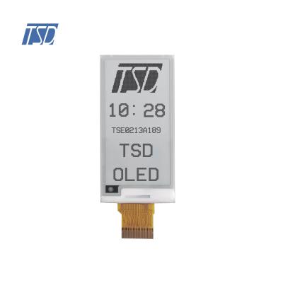
TSE0213A189 is an Active Matrix Electrophoretic Display (AMEPD), with interface and a reference system design. The 2.13’’ active area contains 122×250 pixels,
and has 1-bit B/W full display capabilities. An integrated circuit contains gate buffer, source buffer, interface, timing control logic, oscillator,
DC, SRAM, LUT, VCOM and border are supplied with each panel.
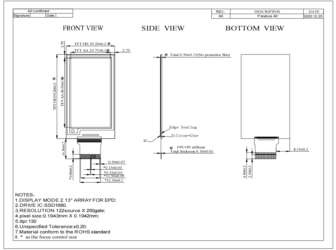
Drawing:
Specifications:
| General Specification | ||
| Part No. | TSE0213A189 | |
| Outline Dimension(mm) |
29.2x59.2x0.9 |
|
| Active Area(mm) | 23.71x48.55 | |
| Resolution(dots) | 122x250 | |
| Operating temperature(°C) | 0 ~ +40°C | |
| Storage temperature(°C) | 0 ~ +50°C | |
| Pin Number | 24pins | |
| Touch panel | without | |
| Driver IC | SSD1680 | |
| Pixel arrangement | RGB-stripe | |
| Display mode | High Contrast 2.13 inch E-ink Display | |
| DPI | 130 | |
| Weight(g) | TBD | |
| Power Consumption(w) | Panel | TBD(Typ.) |
| B/L system | TBD(Typ.) | |
| Interface | I2C | |
| Module lifetime(Hours) | 30,000 hours | |
| Pins Description | ||
| Pin No. | Symbol | Description |
| 1 | NC | No connection and do not connect with other NC pins |
| 2 | GDR | N-Channel MOSFET Gate Drive Control |
| 3 | RESE | Current Sense Input for the Control Loop |
| 4 | NC | No connection and do not connect with other NC pins |
| 5 | VSH2 | Positive Source driving voltage |
| 6 | TSCL | I²C Interface to digital temperature sensor Clock pin |
| 7 | TSDA | I²C Interface to digital temperature sensor Data pin. |
| 8 | BSI | Bus selection pin |
| 9 | BUSY | Busy state output pin |
| 10 | RES# | Reset Signal Input |
| 11 | D/C# | Data /Command control pin |
| 12 | CS# | The chip selects input connecting to the MCU. |
| 13 | SCL | Serial clock pin for interface. |
| 14 | SCL | Serial data pin for interface. |
| 15 | SCL | Power input pin for the Interface. |
| 16 | SCL | Power Supply pin for the chip |
| 17 | SCL | Ground (Digital) |
| 18 | SCL | Core logic power pin |
| 19 | SCL | Power Supply for OTP Programming |
| 20 | SCL | Positive Source driving voltage |
| 21 | SCL | Power Supply pin for Positive Gate driving voltage and VSH |
| 22 | SCL | Negative Source driving voltage |
| 23 | SCL | Power Supply pin for Negative Gate driving voltage, VCOM and VSL |
| 24 | SCL | VCOM driving voltag |
Other Features of E-ink Display:
High contrast
High reflectance
Ultra wide viewing angle
Ultra low power consumption
Pure reflective mode
Bi-stable display
Commercial temperature range
Landscape, portrait modes
Hard-coat antiglare display surface
Ultra Low current deep sleep mode
On-chip display RAM
Low voltage detect for supply voltage
High voltage ready detect for driving voltage
Internal temperature sensor
10-byte OTP space for module identification
Waveform stored in On-chip OTP
Serial peripheral interface available
On-chip oscillator
On-chip booster and regulator control for generating VCOM, Gate and Source driving voltage
I2C signal master interface to read external temperature sensor/ built-in temperature sensor
Applications:
2.13'' Eink Display used for Electronic Shelf Label System.