Email : info@tslcd.com
 Tel : +86-755-28225963


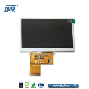
Description:
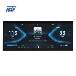
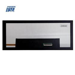
TST103HDKK-02 is 10.3 inch IPS tft lcd display, this is a color active matrix thin film transistor (TFT) liquid crystal display (LCD)that uses a-Si and transmissive TFT as a switching device with normal-black technology. It is composed of a TFT LCD panel, driver IC and back-light. The TFT LCD has10.3 inch with 1920 x 720 resolution and RoHS directive.
Drawing:
Specifications:
| General Specification | ||
| Part No. | TST103HDKK-02 | |
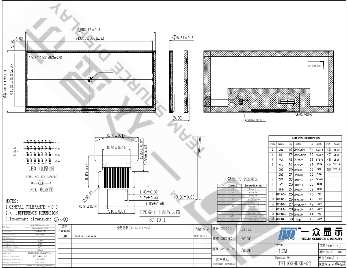
| Outline Dimension(mm) | 253.15x106.01x6.81mm | |
| Active Area(mm) | 243.65x91.37mm | |
| Resolution(dots) | 1920x720 | |
| Operating temperature(°C) | -40 ~ +85°C | |
| Storage temperature(°C) | -40 ~ +90°C | |
| Number of Pixel(pixels) | 1920(H)xRGBx720(V) | |
| Touch panel | without | |
| Brightness | 1000 cd/m2 | |
| Pixel arrangement | RGB-stripe | |
| Display mode | Normal black,IPS, 10.3 inch TFT | |
| Surface treatment | Antiglare | |
| View direction | All |
|
| Weight(g) | TBD | |
| Power Consumption(w) | Panel | TBD(Typ.) |
| B/L system | TBD(Typ.) | |
| Interface | LVDS | |
| Module lifetime(Hours) | 30,000 | |
| Pins Description | ||
| Pin No. | Symbol | Description |
| 1 | GND | Ground |
| 2 | BIST | LCD Panel Self Test Enable, When it is not used, connecting to GND is recommended, don't floating |
| 3 | VCC | Digital PowerVin = 3.3V |
| 4 | VCC | Digital PowerVin = 3.3V |
| 5 | GND | Ground |
| 6 | GND | Ground |
| 7 | OTP | Serial interface OTP power |
| 8 | NC | No connection |
| 9 | GND | Ground |
| 10 | ORXIN0- | Negative LVDS differential data input(Odd data) |
| 11 | ORXIN0+ | Postive LVDS differential data input(Odd data) |
| 12 | ORXIN1- | Negative LVDS differential data input(Odd data) |
| 13 | ORXIN1+ | Postive LVDS differential data input(Odd data) |
| 14 | ORXIN2- | Negative LVDS differential data input(Odd data) |
| 15 | ORXIN2+ | Postive LVDS differential data input(Odd data) |
| 16 | ORXCLKIN- | Negative LVDS differential data input(Odd clock) |
| 17 | ORXCLKIN+ | NegativePositive LVDS differential data input(Odd clock) |
| 18 | ORXIN3- | Negative LVDS differential data input(Odd data) |
| 19 | ORXIN3+ | Postive LVDS differential data input(Odd data) |
| 20 | ERXIN0- | Negative LVDS differential data input(Even data) |
| 21 | ERXIN0+ |
Positive LVDS differential data input(Even data) |
| 22 | ERXIN1- |
Negative LVDS differential data input(Even data) |
| 23 | ERXIN1+ | Positive LVDS differential data input(Even data) |
| 24 | ERXIN2- |
Negative LVDS differential data input(Even data) |
| 25 | ERXIN2+ |
Postive LVDS differential data input(Even data) |
| 26 | ERXCLKIN- | Negative LVDS differential data input(Even clock) |
| 27 | ERXCLKIN+ | Postive LVDS differential data input(Even clock) |
| 28 | ERXIN3- | Negative LVDS differential data input(Even data) |
| 29 | ERXIN3+ | Postive LVDS differential data input(Even data) |
| 30 | GND | Ground |
| 31 | FAULT | FAULT signal output(normal=H, abnormal=L) |
| 32 | RESET | Global reset pin, active High |
| 33 | STBYB | Standby mode, active High |
| 34 | CSB | Serial interface chip enable |
| 35 | SCL | Serial interface clock input |
| 36 | SDAI | Serial interface data input |
|
37 |
SDAO | Serial interface data output |
| 38 | GND | Ground |
| 39 | GND | Ground |
| 40 | NC | No connect |
| 41 | GND | LED power(Anode) |
| 42 | Link2-NC | LED power(Anode) |
| 43 | GND | LED power(Anode) |
| 44 | NC | No connect |
| 45 | LEDK | Cathode1 |
| 46 | LEDK | Cathode2 |
| 47 | LEDK | Cathode3 |
| 48 | LEDK | Cathode4 |
| 49 | NTC_A | NTC_Anode |
| 50 | NTC_K | NTC_Cathode |
Features:
• Display Resolution: 1920 x RGB x 720
• Wide viewing angle (U/D/L/R): Free viewing direction
• Display up to 16.7M colours
LVDS interface
• Anti-glare front polarizer and front polarizer absorption axis angle is horizontal, rear polarizer absorption axis angle is vertical.
• White LED backlight
• “RoHS” compliance.